ME Assistant Professor Xiaogan Liang and ME Professor Wei Lu’s research has been published in Microsystems & Nanoengineering, which is the first engineering-oriented journal under the Nature Publishing Group. Their paper is titled “Scaling behavior of nanoimprint and nanoprinting lithography for producing nanostructures of molybdenum disulfide.” ME PhD students Mikai Chen and Hossein Rokni were co-authors on the paper.
Liang and Lu’s paper was also selected by the Special Topic Session – Nanomanufacturing feature. Despite a large and growing volume of papers on nanotechnology, commercialization of these technologies has been restricted by the lack of driving applications, and the ability to produce nanotechnologies at scale. The Nanomanufacturing Special Topic Session addresses the second of these challenges, by examining the state of “nanomanufacturing”, reviewing a commercial success in the field, and introducing processes that have promise for mass production. Liang and Lu’s paper is one of seven invited papers.
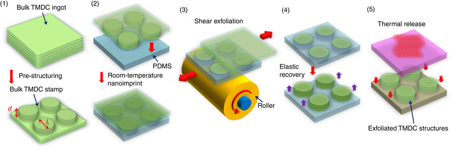
The abstract for their paper reads as follows: “Top-down lithography techniques are needed for manufacturing uniform device structures based on emerging 2D-layered materials. Mechanical exfoliation approaches based on nanoimprint and nanoprint principles are capable of producing ordered arrays of multilayer transition metal dichalcogenide microstructures with a high uniformity of feature dimensions. In this study, we present a study on the applicability of nanoimprint-assisted shear exfoliation for generating ultrathin monolayer and few-layer MoS2 structures as well as the critical limits of feature dimensions produced via such nanoimprint and nanoprint-based processes. In particular, this work shows that give a lateral feature size of MoS2 structures that are pre-patterned on a bulk stamp, there exists a critical thickness or aspect ratio value, below which the exfoliated layered structures exhibit major defects. To exfoliate a high-quality, uniform monolayer or few-layer structures, the characteristic lateral feature sizes of such structures need to be in the sub-100 nm regimes. In addition, the exfoliated MoS2 flakes of critical thicknesses exhibit prominent interlayer twisting features on their cleaved surfaces. Field-effect transistors made from these MoS2 flakes exhibit multiple (or quasi-analog-tunable) charge memory states. This work advances the knowledge regarding the limitations and application scope of nanoimprint and nanoprint processes in manufacturing nano/microstructures based on layered materials and provides a method for producing multi-bit charge memory devices.”