Professor Wei Lu and PhD student Hossein Rokni’s research into one of the strongest materials on earth, graphene, helps in the progress of the development of the graphene and other newly-emerged atomically thin layered materials (e.g., MoS2, WS2, MoSe2, MoTe2, etc.) in (bio)electronic devices including flexible biosensors, transparent touchscreen displays, high-storage, fast-charging batteries, flexible ultrafast transistors and solar cells.
In particular, recent studies have shown that both monolayer graphene and few-layer graphene (formed by vertically stacking monolayer graphene through weak van der Waals interaction) display unique electrical, mechanical, electrochemical, and optical properties that are not essentially observed in their bulk graphite. However, turning the bulk graphite into mono- and few-layer graphene as an essential building block for the new generation of high-performance micro- and nanoelectronic devices has still remained challenging.
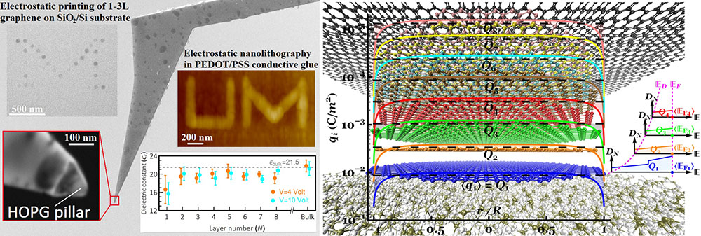
As a means to address such a challenging issue, the team exploited for the first time an in-situ flattened, and conductive atomic force microscopy tip with an attached nanosized graphite pillar to reliably produce high-quality mono- and few-layer graphene features of different shapes and sizes at significant yields. This unique nanoscale manipulation setup with ultrahigh force-displacement resolution allowed them to successfully produce The University of Michigan’s thinnest possible logo by only mono-, bi- and trilayer graphene flakes. They also implemented, for the first time, 3D spatial charge distribution of layered materials into molecular dynamics simulations to further reveal the anisotropic nature of the van der Waals interactions in the layered materials for accurate control of the number of exfoliated flakes. Their experimental observations and atomistic simulations showed that the shear exfoliation technique exhibits a very promising and controllable behavior during the exfoliation process by eliminating the interlayer spacing variations and consequently suppressing the interlayer twist angles.
The setup also allowed the researchers to quantify, for the first time, the effect of layer number and electric field on the dielectric constant of few-layer graphene. Despite the importance of such a fundamental property for any electronic material, there have been very limited studies with significant diversity in the reported values of the dielectric constant of graphitic systems. Surprisingly, however, there is no direct experimental evidence for the dependence of the dielectric constant of few-layer graphene on the layer number and the electric field. As such, they performed a series of dielectric measurements on the one-to-eight layers of graphene under ambient conditions and successfully showed that although the dielectric screening ability of monolayer graphene is about 20% weaker than that of bulk graphite, the overall dielectric response of few-layer graphene samples is almost independent of the number of layers and the external electric field, which is well consistent with their spatial charge distribution model. Due to unexpectedly large variations in the screening ability of pristine monolayer graphene under ambient conditions, they further showed that the effective dielectric constant of monolayer graphene can be engineered to provide a broad spectrum of dielectric responses through oxidation and thermal annealing, which makes it an excellent electric field and charge screening material upon oxidation and recover its charge storage capability upon thermal annealing. Surprisingly, however, bilayer graphene and few-layer graphene can maintain their chemical inertness under oxidation and thus are a better choice for fabrication of long-term stable electronic devices with higher moisture and oxidation resistance.
Their findings about the complex behavior of the van der Waals interactions between the graphene layers and the way the interlayer shear and normal bond breakings change, is a general and fundamental result and thus can be used for various types of exfoliation techniques. While they have specifically focused on the few-layer graphene systems, their analyses should be extensible to the exfoliation of other newly emerged thin layered materials, leading to the effective production of two-dimensional materials for use in high-performance thin layered material–based electronic and mechanical devices. This work, titled “Nanoscale Probing of Interaction in Atomically Thin Layered Materials”, has been recently published in ACS Central Science and attracted media attention.
